- 您现在的位置:买卖IC网 > Sheet目录335 > ISL89410IBZ-T13 (Intersil)IC DRVR MOSFET DUAL-CH 8-SOIC
�� �
�
�ISL89410,� ISL89411,� ISL89412�
�.subckt� comp1� out� inp� inm� vss�
�e1� out� vss� table� {� (v(inp)� v(inm))*� 5000}� (0,0)� (3.2,3.2)�
�Rout� out� vss� 10meg�
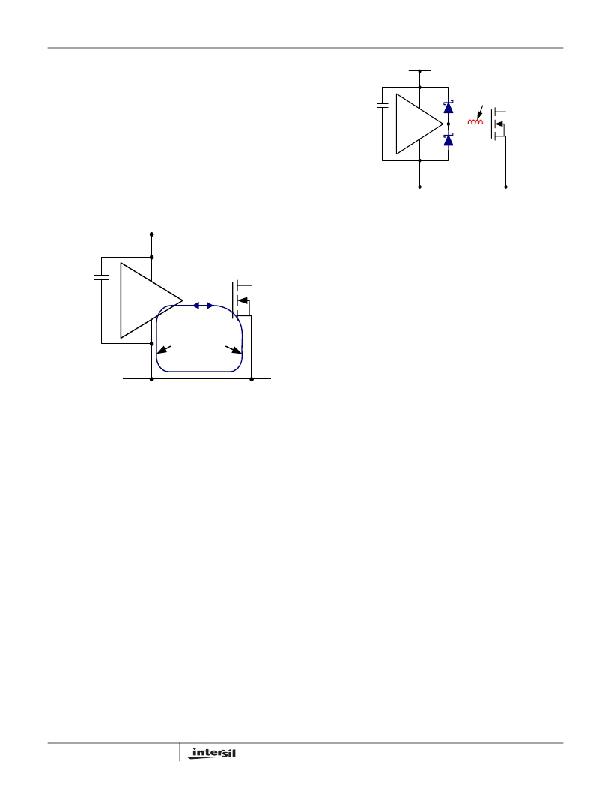
�V+�
�Rinp� inp� vss� 10meg�
�Rinm� inm� vss� 10meg�
�.ends� comp1�
�Application� Guidelines�
�It� is� important� to� minimize� inductance� to� the� power� FET� by�
�keeping� the� output� drive� current� loop� as� short� as� possible.�
�Also,� the� decoupling� capacitor,� Cq,� should� be� a� high� quality�
�ceramic� capacitor� with� a� Q� that� should� be� a� least� 10x� the�
�gate� Q� of� the� power� FET.� A� ground� plane� under� this� circuit� is�
�C� q�
�GND�
�PARASITIC� LEAD�
�INDUCTANCE�
�also� recommended.�
�C� q�
�V+�
�C� q� SHOULD� BE� AS� CLOSE� AS�
�POSSIBLE� TO� THE� V+� AND�
�GND� PINS�
�LOOP� AS�
�FIGURE� 15.� SUGGESTED� CONFIGURATION� FOR� DRIVING�
�INDUCTIVE� LOADS�
�Where� high� supply� voltage� operation� is� required� (15V� to�
�18V),� input� signals� with� a� minimum� of� 3.3V� input� drive� is�
�suggested� and� a� minimum� rise/fall� time� of� 100ns.� This� is�
�recommended� to� minimize� the� internal� bias� current� power�
�dissipation.�
�Excessive� power� dissipation� in� the� driver� can� result� when�
�driving� highly� capacitive� FET� gates� at� high� frequencies.�
�These� gate� power� losses� are� defined� by� Equation� 1:�
�SHORT� AS�
�POSSIBLE�
�GND�
�FIGURE� 14.� RECOMMENDED� LAYOUT� METHODS�
�P� =� 2� ?� Q� C� ?� V� gs� ?� f� SW�
�where:�
�P� =� Power�
�Q� c� =� Charge� of� the� Power� FET� at� V� gs�
�(EQ.� 1)�
�In� applications� where� it� is� difficult� to� place� the� driver� very�
�close� to� the� power� FET� (which� may� result� with� excessive�
�parasitic� inductance),� it� then� may� be� necessary� to� add� an�
�external� gate� resistor� to� dampen� the� inductive� ring.� If� this�
�resistor� must� be� too� large� in� value� to� be� effective,� then� as� an�
�alternative,� Schottky� diodes� can� be� added� to� clamp� the� ring�
�voltage� to� V+� or� GND.�
�8�
�V� gs� =� Gate� drive� voltage� (V+)�
�f� SW� =� switching� Frequency�
�Adding� a� gate� resistor� to� the� output� of� the� driver� will� transfer�
�some� of� the� driver� dissipation� to� the� resistor.� Another�
�possible� solution� is� to� lower� the� gate� driver� voltage� which�
�also� lowers� Q� c� .�
�FN6798.1�
�July� 1,� 2009�
�发布紧急采购,3分钟左右您将得到回复。
相关PDF资料
ISL9440AEVAL1Z
EVALUATION BOARD FOR ISL9440
ISL9440BEVAL1Z
EVAL BOARD 1 FOR ISL9440B
ISL97631IHTZ-T7
IC LED DRIVR WHITE BCKLGT TSOT-6
ISL97634IRT26Z-TK
IC LED DRIVR WHITE BCKLGT 8-TDFN
ISL97635AIRZ
IC LED DRVR WHT/RGB BCKLGT 24QFN
ISL97635IRZ
IC LED DRVR WHT/RGB BCKLGT 24QFN
ISL97636AIRZ
IC LED DRIVR WHITE BCKLGT 24-QFN
ISL97636IRZ-TK
IC LED DRIVR WHITE BCKLGT 24-QFN
相关代理商/技术参数
ISL89410IP
功能描述:IC DRVR MOSFET DUAL-CH 8-PDIP RoHS:否 类别:集成电路 (IC) >> PMIC - MOSFET,电桥驱动器 - 外部开关 系列:- 标准包装:50 系列:- 配置:低端 输入类型:非反相 延迟时间:40ns 电流 - 峰:9A 配置数:1 输出数:1 高端电压 - 最大(自引导启动):- 电源电压:4.5 V ~ 35 V 工作温度:-40°C ~ 125°C 安装类型:表面贴装 封装/外壳:TO-263-6,D²Pak(5 引线+接片),TO-263BA 供应商设备封装:TO-263 包装:管件
ISL89410IPZ
功能描述:IC DVR MOSFET DUAL-CH 8-PDIP RoHS:是 类别:集成电路 (IC) >> PMIC - MOSFET,电桥驱动器 - 外部开关 系列:- 标准包装:6,000 系列:*
ISL89411IBZ
功能描述:功率驱动器IC DUAL INVERT DRVR MODIFIED EL7212 8LD RoHS:否 制造商:Micrel 产品:MOSFET Gate Drivers 类型:Low Cost High or Low Side MOSFET Driver 上升时间: 下降时间: 电源电压-最大:30 V 电源电压-最小:2.75 V 电源电流: 最大功率耗散: 最大工作温度:+ 85 C 安装风格:SMD/SMT 封装 / 箱体:SOIC-8 封装:Tube
ISL89411IBZ-T13
功能描述:IC DRVR MOSFET DUAL-CH 8-SOIC RoHS:是 类别:集成电路 (IC) >> PMIC - MOSFET,电桥驱动器 - 外部开关 系列:- 标准包装:5 系列:- 配置:低端 输入类型:非反相 延迟时间:600ns 电流 - 峰:12A 配置数:1 输出数:1 高端电压 - 最大(自引导启动):- 电源电压:14.2 V ~ 15.8 V 工作温度:-20°C ~ 60°C 安装类型:通孔 封装/外壳:21-SIP 模块 供应商设备封装:模块 包装:散装 配用:BG2A-NF-ND - KIT DEV BOARD FOR IGBT 其它名称:835-1063
ISL89411IP
制造商:Intersil Corporation 功能描述:
ISL89411IPZ
功能描述:IC DRVR MOSFET DUAL-CH 8-PDIP RoHS:是 类别:集成电路 (IC) >> PMIC - MOSFET,电桥驱动器 - 外部开关 系列:- 标准包装:6,000 系列:*
ISL89412IBZ
功能描述:功率驱动器IC COMP MOSFET DRVR MODIFIED EL7222 8LD RoHS:否 制造商:Micrel 产品:MOSFET Gate Drivers 类型:Low Cost High or Low Side MOSFET Driver 上升时间: 下降时间: 电源电压-最大:30 V 电源电压-最小:2.75 V 电源电流: 最大功率耗散: 最大工作温度:+ 85 C 安装风格:SMD/SMT 封装 / 箱体:SOIC-8 封装:Tube
ISL89412IBZ-T13
功能描述:IC DRVR MOSFET DUAL-CH 8-SOIC RoHS:是 类别:集成电路 (IC) >> PMIC - MOSFET,电桥驱动器 - 外部开关 系列:- 标准包装:5 系列:- 配置:低端 输入类型:非反相 延迟时间:600ns 电流 - 峰:12A 配置数:1 输出数:1 高端电压 - 最大(自引导启动):- 电源电压:14.2 V ~ 15.8 V 工作温度:-20°C ~ 60°C 安装类型:通孔 封装/外壳:21-SIP 模块 供应商设备封装:模块 包装:散装 配用:BG2A-NF-ND - KIT DEV BOARD FOR IGBT 其它名称:835-1063